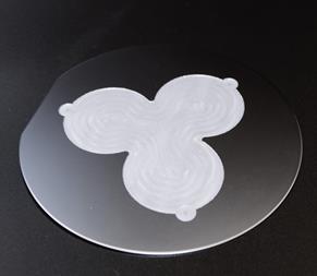
Polishing / Grinding / Cutting
Packaging, polishing, and CMP for polishing.。Grinder polishing。
Cutting using slicing and chunking。
We process to meet all shapes and required precision 。
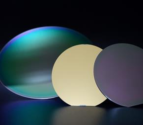
| Types | Manufacturing Methods | Film-type |
|---|---|---|
| 氧化膜系統 | hermal Oxide Film | Thin Thermal Oxide Film |
| Ultra-thick Thermal Oxide Film | ||
| Low-Pressure Chemical Vapor Deposition | LP-SiO2、HTO、LP-TEOS | |
| PE-CVD | PE-SiO2、PE-TEOS、HDP、Low-k(BD、BDⅡ、AURORA、CORAL)、PSG、NSG、BPSG | |
| Spin Coating | Sog | |
| Annealing Furnace | RTO | |
| Nitride Film System | Low-Pressure Chemical Vapor Deposition | LP-SiN |
| PE-CVD | PE-SiN | |
| Si Film | Low-Pressure Chemical Vapor Deposition | Polycrystalline Silicon |
| Polycrystalline Silicon/font> | ||
| Organic Film System | Spin Coating | G-line Photoresist, I-line Photoresist, KrF Photoresist, ArF Photoresist, Polyimide (photosensitive, non-photosensitive) |
| Metal Type | Sputtering | Al、Al-Si、Al-Si-Cu、Al-Cu、Ti、TiN、Ta、TaN、Cr、Cu、W、Ni、Au、Pt、ITO等 |
| Electroplating | Titanium, Nickel, Gold, Copper, etc | |
| Chemical Vapor Deposition | Tungsten Silicon |
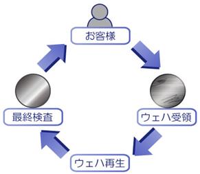
| Play Type | Reclaimable Film Species | Size | Minimum Quantity |
|---|---|---|---|
| Polishing Reclamation | Excluding precious metals like Gold, Copper, Platinum, etc | φ3”to φ8” | 25 sheets |
| Chemical Reclamation | Excluding precious metals like Gold, Copper, Platinum, etc | φ3”to φ8” | 25 sheets |